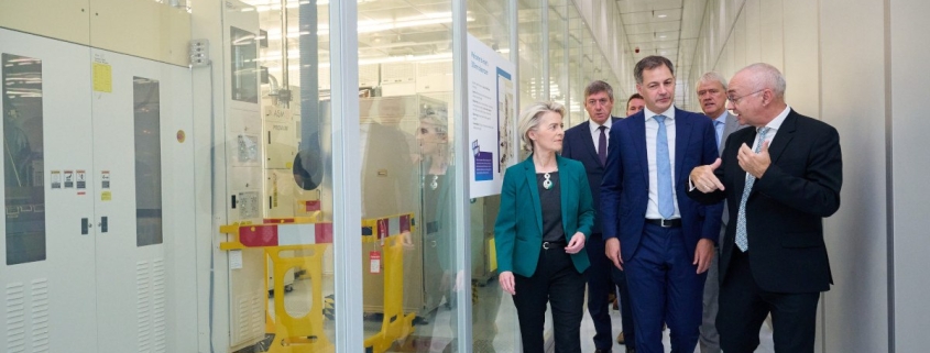
€2.5bn EU NanoIC pilot line launched to usher in next-gen chips
Europe’s Semiconductor Future Just Got a Major Boost with the Launch of the €2.5bn NanoIC Pilot Line
In a monumental stride toward global semiconductor supremacy, the European Union has officially unveiled the NanoIC pilot line, a cutting-edge facility poised to catapult Europe into the forefront of next-generation chip technology. Launched today at the Interuniversity Microelectronics Centre (Imec) in Leuven, Belgium, this €2.5bn initiative represents the largest investment under the EU Chips Act, signaling Europe’s unwavering commitment to securing its place in the highly competitive semiconductor industry.
A Game-Changer for European Innovation
The NanoIC pilot line is the crown jewel of the EU Chips Act, which has allocated a staggering €3.7bn across five pilot lines: Fames, Apecs, WBG, PixEurope, and NanoIC. These facilities are designed to bridge the gap between laboratory research and industrial-scale production, ensuring that groundbreaking innovations in chip technology can transition seamlessly from concept to reality.
NanoIC, in particular, is set to revolutionize the semiconductor landscape. With €700m in EU funding, €700m from national and regional governments, and additional contributions from industry giants like ASML, the facility is equipped to accelerate the development of chips beyond the 2nm threshold. This marks a significant leap forward, as the facility will be the first in Europe to deploy advanced extreme ultraviolet (EUV) lithography technology, a game-changing innovation that uses light with wavelengths as short as 13.5nm to print microchips.
A Collaborative Effort for Global Leadership
The NanoIC facility is not just a technological marvel; it is a testament to the power of collaboration. Hosted at Imec, the pilot line is supported by a consortium of leading research institutions, including Tyndall National Institute in Ireland, CEA in France, Fraunhofer-Gesellschaft in Germany, VTT Technical Research Centre in Finland, and Romania’s Centre for Surface Science and Nanotechnology. This diverse partnership underscores the EU’s commitment to fostering innovation through collective expertise and shared resources.
Tyndall National Institute, a key partner in the NanoIC initiative, has been making waves in the semiconductor world. Just last month, the institute announced an ambitious €100m expansion plan aimed at doubling its organizational footprint and solidifying Ireland’s position as a global hub for semiconductor research and development. This expansion, coupled with Tyndall’s involvement in NanoIC, positions Ireland as a critical player in Europe’s semiconductor strategy.
A Strategic Move in the Global Semiconductor Race
The launch of NanoIC comes at a pivotal moment in the global semiconductor industry. Nearly four years after the EU Chips Act was first announced in 2022, and just months after EU member states endorsed the ‘Semiconductor Declaration,’ the initiative reflects Europe’s determination to reduce its reliance on non-European chip manufacturers and bolster its own semiconductor ecosystem.
The Semiconductor Declaration, which recognizes the critical importance of semiconductors for the EU’s competitiveness and resilience, also sets the stage for the upcoming revision of the European Chips Act, dubbed ‘Chips Act 2.0.’ This revision aims to further strengthen Europe’s semiconductor capabilities, ensuring that the continent remains at the forefront of technological innovation.
The Road Ahead: From Lab to Fab
The NanoIC pilot line is more than just a facility; it is a gateway to the future of semiconductor technology. By providing access to state-of-the-art equipment and fostering collaboration between start-ups, researchers, SMEs, and large organizations, NanoIC is poised to drive innovation at an unprecedented scale. The facility’s focus on advanced EUV lithography and sub-2nm chip technology positions it as a critical enabler of next-generation applications, from artificial intelligence and quantum computing to autonomous vehicles and beyond.
As the world becomes increasingly reliant on semiconductor technology, the EU’s investment in NanoIC and the broader Chips Act initiative sends a clear message: Europe is ready to lead the charge in shaping the future of technology. With its cutting-edge infrastructure, collaborative ecosystem, and unwavering commitment to innovation, the NanoIC pilot line is set to redefine the boundaries of what is possible in the semiconductor industry.
Tags: #EU #Semiconductors #NanoIC #ChipsAct #Innovation #ASML #EUV #TyndallNationalInstitute #Imec #Technology #FutureOfTech #GlobalLeadership #ResearchAndDevelopment #Microelectronics #NextGenChips #SemiconductorIndustry #EUInnovation #TechNews #BreakthroughTechnology #SemiconductorDeclaration #ChipsAct2.0
Viral Phrases: “Europe’s semiconductor supremacy,” “Next-gen chip technology,” “From lab to fab,” “Cutting-edge EUV lithography,” “Global semiconductor race,” “Collaborative innovation,” “Shaping the future of tech,” “Unprecedented scale of innovation,” “Critical enabler of next-gen applications,” “Redefining the boundaries of technology.”
,


Leave a Reply
Want to join the discussion?Feel free to contribute!